Trollbook: The Struggles (part 1)
When designing any project, even vaguely advanced, you're bound to make mistakes. Especially if it's something you've never done before. Trollbook sure was something new for us.
1 Initial Bringup
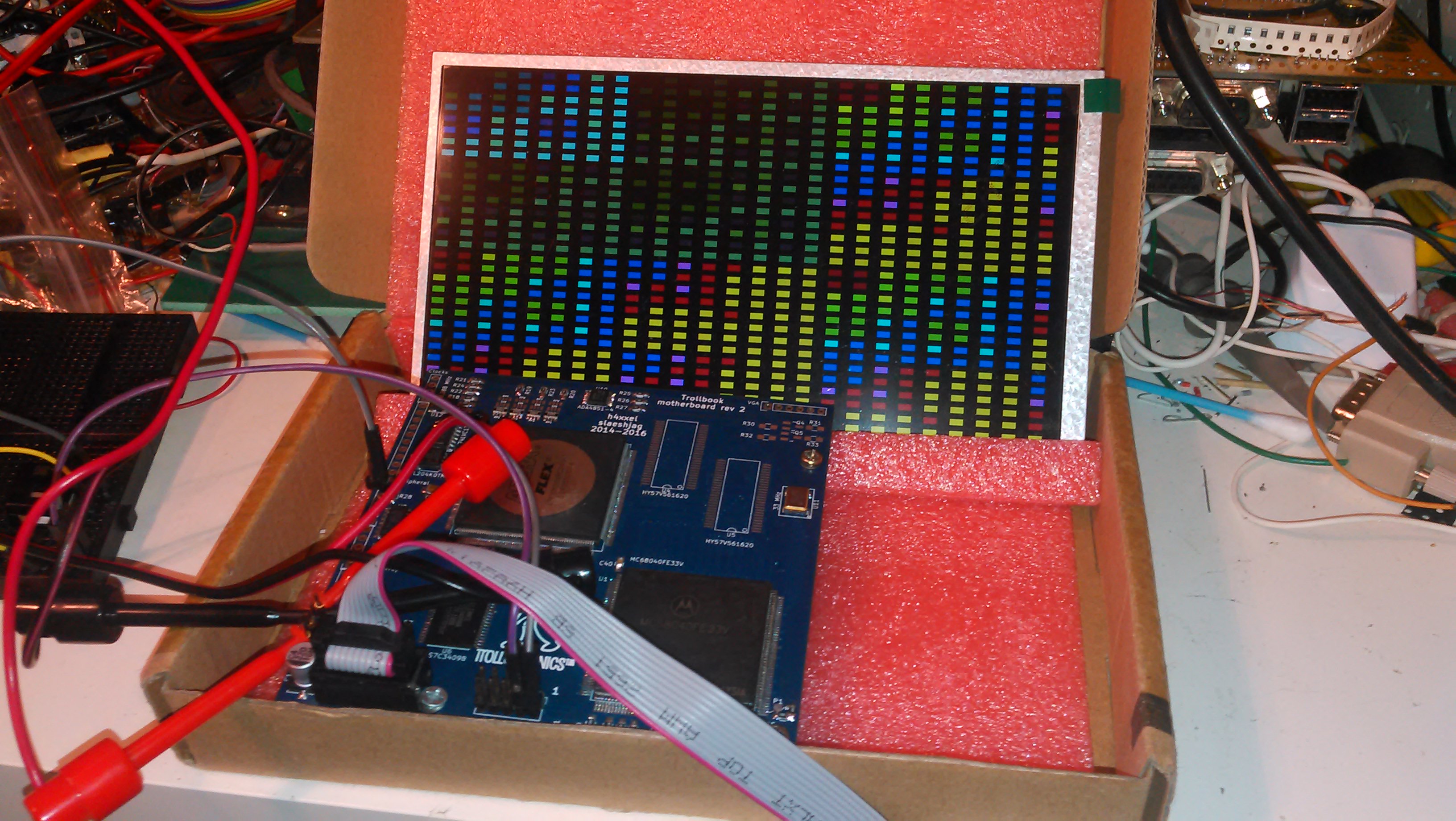
Ok, so we designed the mainboard. We got the components. After double-checking, tripple-checking, and quadruple-checking everything, we finally ordered the PCB. 4 layers, 10x10cm, it cost us $45 + shipping, more than we've ever spent on a PCB. FPGA, SRAM, CPU and passives to go with it was soldered on. The LCD connected and h4xxel started with pushing a simple demo to the FPGA to generate color patterns on the screen. This is a promising start, at least the FPGA is vaguely working.
So, next up is the CPU. With some fairly simple bus glue (all reads to internal ROM, all writes to framebuffer), we got the CPU up and running too, generating color patterns. Next up, a UART was implemented on the FPGA to send over a full-screen picture. This is where the first problem started. There was some strange data corruption on the framebuffer. But that later turned out to be a few address pins on the CPU not being soldered down properly. Oops.
Another issue we faced was reading back data from the SRAM. We managed to write data fine as evident by our framebuffer tests, but the data we got back was mostly garbage, although seemingly related to what was on screen. This later turned out to be a hold-time violation. The propagation time from the SRAM to its outputs, and from the FPGA's input to its internal flip-flops was too long for the half-clock cycle we were waiting for the data. After faffing about with the HDL, we now got it waiting the full clock like it should, and data is reading fine. This means we can send code from the serial port to the SRAM and execute it from there.
Another minor issue we faced was a very temperamental UART. It worked sometimes, but not always. After replacing all connectors with just soldered down pin-headers there was still problems with recieving data on the serial port. This later turned out to be a bad soldering joint on the FPGA. It's amazing how bad soldering can cause such intermittent issues.
2 The SDRAM
About this now, the SDRAM was the next item on the list of hardware to bring up. Once we got the SDRAM running, we can start writing or porting a real operating system to run on our computer, and that would really exciting, as it would be like a real computer, not just a toy! The SDRAM also cause the most headaches this far. It stalled us for several months. While the basic operations are quite simple, with a small state-machine at init writing a few commands, making sure to issue a refresh command often enough and not to keep banks/rows/columns open for too long, and it should all be fine.
At first, we could read nothing but 0xFFFFFFFF. Burst reads would lock up the bus and all of those other fun problems. We had access to a logic analyzer that can do 33 MHz no problem, but the didn't have clips that would comfortably attach to a 0.65mm pitch TSOP. Two next to each other would often cause shorts. Eventually, h4xxel designed and soldered up a separate board with just an SDRAM, a Xilinx 9572 CPLD and a clock. And a 0.1" pin header with a pin for every signal. With this setup, hooking up a logic analyzer was a breeze and one thing soon became apparent...
In the datasheet for most, if not all SDRAM, it is mentioned how with SDRAM, all signals are latched on rising clock edge. And this is true. The datasheets also makes it look like the data changes on falling edge. This is also true. In some cases. Specifically, when you run the SDRAM at its rated clock speed. You see, the change is not actually synchronized on falling edge. It's just a hold time after rising edge. So 6 or so ns after the rising edge, the data will start to change with the SDRAM we chose. The problem is that our CPU, an MC68040FE33V, wants between 8 and 30 ns hold for its data input when reading. That's pretty much an entre clock cycle. So on paper, it's kindof impossible to get this setup working without fractional phase shifts. But we had one trick to try.
Back when we designed the board, we hadn't properly read the datasheet for the SDRAM. We knew it was synchronous, but not at what clock edges. Since we also wanted to be able to turn off the clock signal to the CPU, we routed the CPU clock through the FPGA. So our last attempt at getting it to work, was to flip the clock phase for the CPU in the FPGA. This should mean the CPU gets maybe 22 or so ns of hold time from the SDRAM on reads. It might just be enough. We tried, and we got data! Apart from some minor goofups, it was seemingly working perfect, and before the day was over, we had code executing from SDRAM.
But it was only really testing the first 256 or so bytes. To make sure it was really working, I wrote a crude memory test program. It would just write a block of memory, overwrite the rest of the RAM with FF, and then read back the original block to make sure it's still there. Step up the block address with a power of two to test all address bits and that was about it. We did get some errors. One of them was an obvious address pin fault on one of the chips, but a quick job with the soldering iron later and that problem was cleared. But we still had another issue. Seemingly after a while, after writing a lot of data, random bytes of data would corrupt a bit. Not a lot, maybe just a few bits flipped here and there. This was a lot harder to debug, but was later found to be a problem in our implementation of the SDRAM controller, the bank select lines weren't used. With a quick patch, the memory test is now going through, so we should have all 64 MB of RAM accessable to us!
3 In the next post...
Next up to write about is bringup of audio, troubleshooting of our UART which works great with the cache off (but misses bytes when the cache is on), and troubleshooting of my FAT driver, which during writes will occasionally corrupt existing files on the SD card.
Comments belong to their respective owners. By posting a comment, you agree and give the right for slaeshjag.org to publish or reject it. Your e-mail address will not be published or disclosed to a 3rd party, and is only used for return correspondance or verifying requests to delete comments.
You need JavaScript enabled to post a comment